Electron Spectro-Microscopy in SFEM
In the SFEM, a well-defined electron-beam emitted from the tip is accelerated towards the surface, inducing the generation of low energy electrons. The intensity of these ejected electrons is used to produce topographic images with high spatial resolution. The sample current is monitored as well as the intensity and the energy of those electrons that manage to escape the tip-sample junction.
Those electrons travelling almost parallel to the surface are collected using a channeltron (CEM) by means of which the total electron yield is recorded (see Figure 2 a) and b).
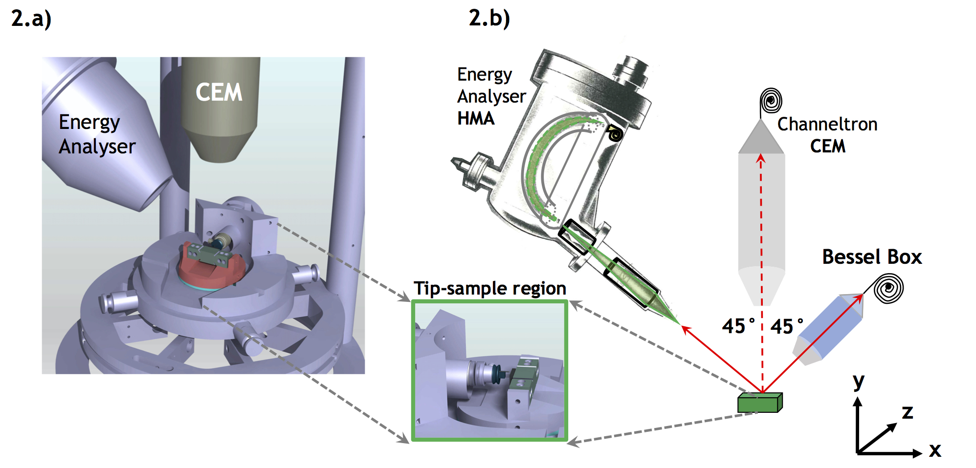
The SFEM instrument in our laboratory was endowed with a conventional hemispherical energy analyzer (HMA, in Figure 2 b).
Scattered and ejected electrons from the surface that manage to escape the tip-sample junction were collected by the HMA and their energy was analyzed, see Figure 3 below.
However, the presence of strong electrostatic fields in the junction region, where the electrons are excited, makes the detection and analysis of the emitted electrons inherently difficult. The strong electric field induces a momentum reversal of the escaping electrons which bounce back towards the surface. This limits their escape and complicates their detection.
To overcome this limitation, we included a prototype miniature electron detection unit, a Bessel Box energy analyzer, into the setup.
Some Results
With our SFEM instrument, the surface topography was investigated by performing an STM-scan, as the one shown in Figure 3 a). The sample area scanned in this figure shows a W(110)-surface covered by Fe-nano-islands (bright spots).
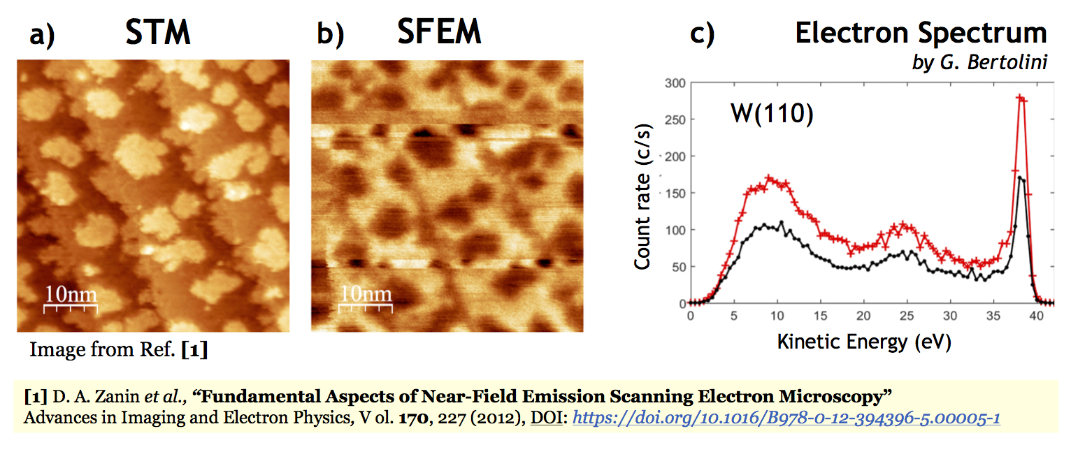
When the tip is retracted and the experiment is then operated in Field-Emission mode, the same area as shown in Figure 3 a) can be scanned in constant height mode, thus obtaining a so-called SFEM image (see Figure 3 b). Here, the image and its contrast are determined by the electrons scattered and ejected from the surface. These electrons are collected by the channeltron. Thus, by doing SFEM-imaging complementary information to STM can be obtained.
Furthermore, these ejected electrons, which penetrate the tip-surface junction, can be collected by our electrostatic hemispherical energy analyzer yielding their energy distribution (Figure 3 c).