Research
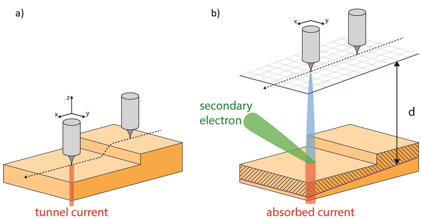
The impact of Scanning Tunneling Microscopy (STM) to nanotechnology continues to be undisputed, but this does not prevent the search for new technologies aiming at potentially revealing aspects complementary to those highlighted by STM. One of these technologies was developed in our research group, within a project sponsored by the European Union (SIMDALEE2: Marie Curie Initial Training Network (ITN), Grant number 606988 under FP7-PEOPLE-2013-ITN) and the Commission for Technology and Innovation (CTI grant number 9860.1 PFNM-NM). This technology, which we called “Scanning Field Emission Microscopy” originates from the “topographiner”. The topografiner was introduced by R. Young at NBS (now NIST-National Institute of Standard and Technology) about 10 years in advance of STM but the method was abandoned because of a management decision. The principle of Scanning Field Emission Microscopy (shortly: SFEM) is schematically illustrated in figure 1.
Figure 1 a) shows a surface (orange) exhibiting terraces separated by a monoatomic step and imaged in the conventional STM mode.
In such an STM scan, the distance between tip (grey) and target is in the subnanometer range, while a small voltage (mV-range) difference is applied between tip and sample. Accordingly, electrons can be exchanged between the atom residing at the apex of the tip and the outermost surface atom by direct quantum mechanical tunneling (Binnig-Rohrer).
The tip is scanned along a horizontal xy-coordinate system while the tunnel current (red) is kept constant by adjusting the distance (in z direction) between the tip and the sample by a feedback loop. Thus, a topographic map of the surface is obtained, with atomic spatial resolution and entailing information on the local density of states. It is this extreme spatial resolution that actually started nanoscience.
In the SFEM mode (Figure 1 b) the tip is retracted away from the surface along the z-axis to a distance, d, of few tens of nanometers (d ~5-50nm) which is kept constant during a scan. At these distances, direct quantum mechanical tunneling between tip and sample is entirely suppressed. Electrons are field emitted from the tip by increasing the tip voltage to negative few tens of Volt and they are both accelerated and focused towards the surface of the target. The field-emitted electrons build the primary-electron beam (blue in Figure 1 b).
Upon striking the target, the primary electrons interact with the solid-state electrons in the target. They are partly absorbed (red in Figure 1 b), but by virtue of elastic and inelastic scattering processes they can be backscattered from the surface and can also give rise to a secondary electron cascade (green in Figure 1 b). Those electrons which are ejected from the target and manage to escape the tip-target junction, thus reaching the macroscopic surrounding, can be analyzed according to their intensity, i.e. producing a “secondary electron image'' of the topography of the target itself. Furthermore, they can be selected according to their energy, enabling spectro-microscopy and alternatively their spin polarization can be analyzed, e.g. producing an image of the magnetic contrast of the target.
The strong electric field between tip and sample focusses the field-emitted electrons onto the target thus inducing a spatially localized primary beam. By the “simple” operation of retracting the tip, the STM turns into a lens-less Low-Energy Scanning Electron Microscope with the possibility to perform secondary-electron imaging, energy and spin analysis.
In the SFEM, a well-defined electron-beam emitted from the tip is accelerated towards the surface, inducing the generation of low energy electrons. The intensity of these ejected electrons is used to produce topographic images with a spatial resolution comparable to that of STM. The sample current is monitored as well as the intensity of those electrons that manage to escape the tip-sample junction.
Those electrons travelling almost parallel to the surface are collected using a channeltron (CEM) by means of which the total electron yield is recorded (see Figure 2 a) and b). Read more about SFEM
The scattering of electrons in solids is dominated by the Coulomb interaction, but electrons have a spin and this degree of freedom affects the scattering processes via two fundamental spin-dependent interactions: the spin-orbit coupling and the exchange interaction.
Electron scattering at surfaces involving spin polarized beams or alternatively the detection of spin-polarization of scattered electrons can be used for various purposes, for instance imaging of the surface magnetic contrast with sub-micrometer spatial resolution.
We are able to analyze the spin polarization of the secondary electrons excited by the primary beam coming from a nanometer-sized tip. These secondary electrons carry information about the local magnetization vector of the target area that resides within the primary beam focus. Read more about polarization analysis

